UB nanotech research getting boost with new electron beam lithography system


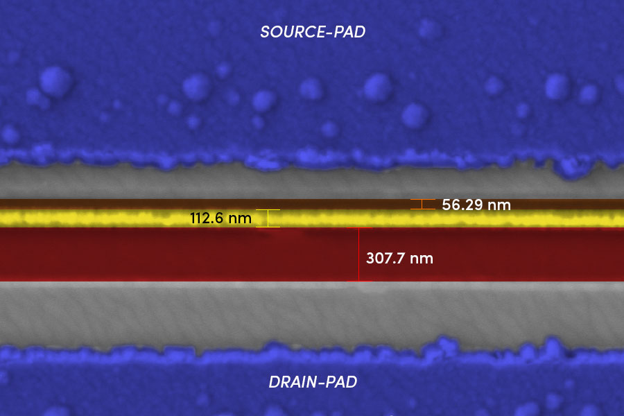
Transistors are the building blocks of computer hardware. Smartphones have billions of them. This image shows a gallium oxide transistor created with an electron beam lithography (EBL) system. The gate (the yellow line) is about 100 nanometers wide — a typical sheet of paper is 100,000 nanometers thick. This is an example of the extremely tiny structures that can be fabricated with EBL systems. Credit: Uttam Singisetti and Abhishek Vaidya, University at Buffalo.
Supported by a $1 million National Science Foundation grant, the system will spur research and economic development in electronics, quantum computing and more
Release Date: November 4, 2019 This content is archived.


BUFFALO, N.Y. — University at Buffalo researchers have received a $1 million National Science Foundation (NSF) grant to help fund the purchase of a new 100-kilovolt electron beam lithography (EBL) system.
A key addition to UB’s research facilities, the system will provide faculty and students, as well as neighboring higher education institutions and tech-minded entrepreneurs in Western New York, access to one of the most advanced tools available to nanotechnology researchers.
“Electron beam lithography is an indispensable tool for nanotechnology research. It has applications in many fields and the potential to rapidly translate knowledge gained in UB’s laboratories to commercial applications,” says the grant’s principal investigator, Uttam Singisetti, PhD, associate professor of electrical engineering in the UB School of Engineering and Applied Sciences.
Rajan Batta, interim dean of the School of Engineering and Applied Sciences, said the system will promote interdisciplinary research and lead to discoveries in electronics, photonics, quantum technology and other fields.
He added: “Tools like this support the region’s economic development efforts, especially in advanced manufacturing and health care, and will help grow the number of tech-savvy workers in Western New York.”
An EBL system is a fabrication tool. It scans a narrow beam of electrons across an electron-sensitive film called a “resist.” The resulting design is developed into template — similar to a stencil — which is then transferred to a substrate material, often by etching. From there, researchers can use the stencil to create extremely fine devices needed for modern electronics, medical devices and other advanced technologies.
The system that UB will acquire allows for the creation of devices less than 10 nanometers thick. (By comparison, a typical sheet of paper is 100,000 nanometers thick.) That’s a significant improvement from UB’s current EBL capabilities, Singisetti says.
Grant co-investigators from the School of Engineering and Applied Sciences include Jonathan Bird, PhD, professor and chair of electrical engineering, and Peter Q. Liu, PhD, assistant professor of electrical engineering.
Additional co-investigators are Sambandamurthy Ganapathy, PhD, professor and chair of physics in the UB College of Arts and Sciences; and Jung-Hun Seo, PhD, assistant professor in the Department of Materials Design and Innovation, a joint program of the School of Engineering and Applied Sciences and College of Arts and Sciences.
In addition to the $1 million from the NSF, UB has set aside $428,571 to help buy the EBL system. The exact tool has not yet been determined because UB is still soliciting quotes from vendors.
The system will be housed within the Davis Hall Clean Room facility on UB’s North Campus, where dozens of UB researchers and hundreds of UB students from at least six departments are expected to utilize it.
“The electron beam lithography system and other cutting-edge research equipment and facilities are essential for recruiting the very best faculty, and undergraduate and graduate students,” says Bird, who added that the EBL system will also help UB to secure additional research funding.
In addition to UB, researchers and students from Rochester Institute of Technology, Alfred State College, SUNY Buffalo State, SUNY Erie Community College and Genesee Community College are expected to use the system.
Media Contact Information
Cory Nealon
Director of Media Relations
Engineering, Computer Science
Tel: 716-645-4614
cmnealon@buffalo.edu