Powerful new photodetector can enable optoelectronics advances


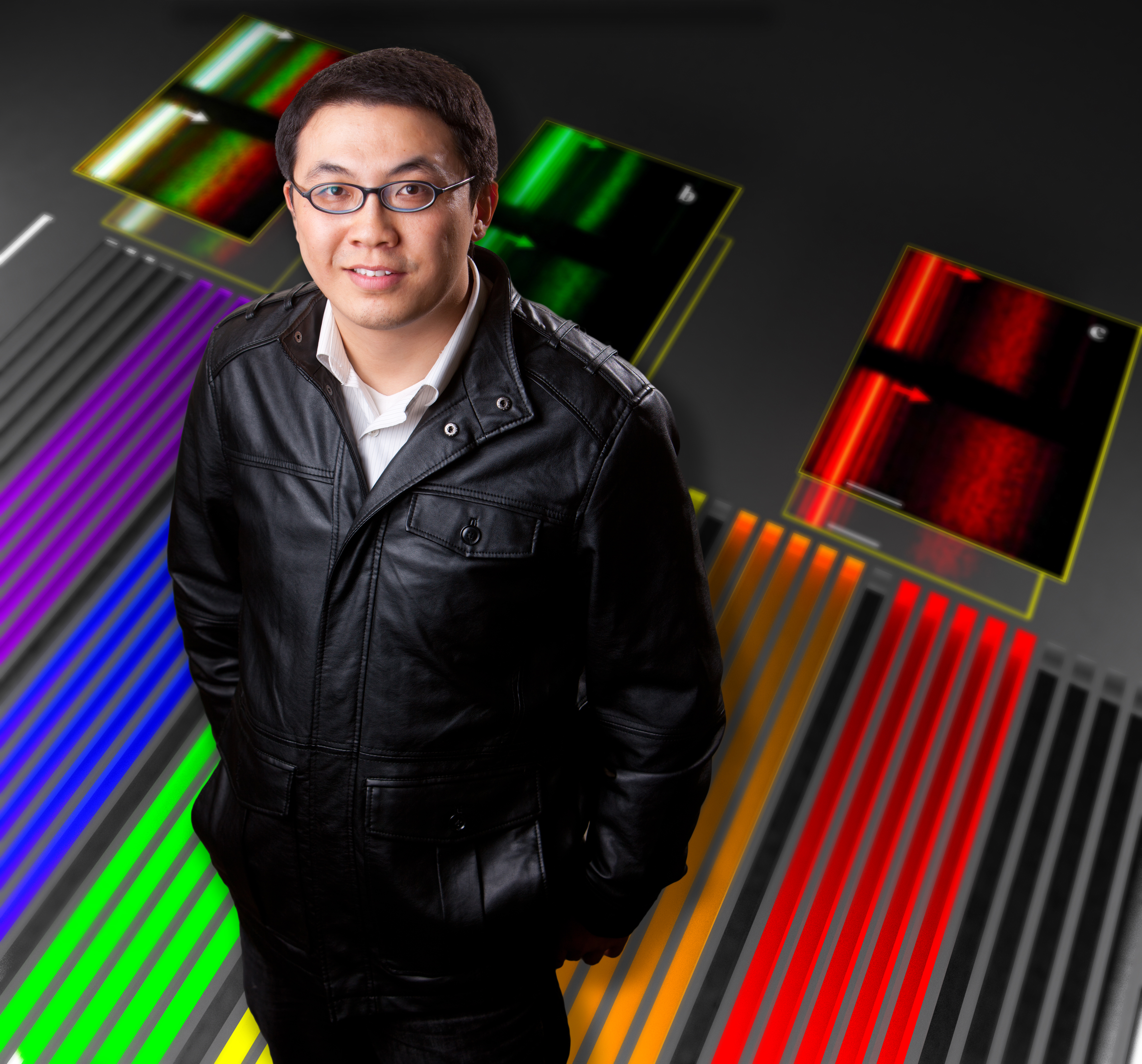
The image shows the different layers of the nanoscale photodetector, including germanium (red) in between layers of gold or aluminum (yellow) and aluminum oxide (purple). The bottom layer is a silver substrate. Credit: University at Buffalo.
The device could improve solar panels, cameras, data sharing and more
Release Date: July 7, 2017 This content is archived.


BUFFALO, N.Y. — In today's increasingly powerful electronics, tiny materials are a must as manufacturers seek to increase performance without adding bulk.
Smaller also is better for optoelectronic devices — like camera sensors or solar cells —which collect light and convert it to electrical energy. Think, for example, about reducing the size and weight of a series of solar panels, producing a higher-quality photo in low lighting conditions, or even transmitting data more quickly.
However, two major challenges have stood in the way: First, shrinking the size of conventionally used “amorphous” thin-film materials also reduces their quality. And second, when ultrathin materials become too thin, they are almost transparent — and actually lose some ability to gather or absorb light.
Now, in a nanoscale photodetector that combines both a unique fabrication method and light-trapping structures, a team of engineers from the University at Buffalo and the University of Wisconsin-Madison has overcome both of those obstacles.
The researchers — electrical engineers Qiaoqiang Gan at UB, and Zhenqiang (Jack) Ma and Zongfu Yu at UW-Madison — described their device, a single-crystalline germanium nanomembrane photodetector on a nanocavity substrate, in the July 7, 2017, issue of the journal Science Advances.
“We’ve created an exceptionally small and extraordinarily powerful device that converts light into energy,” says Gan, associate professor of electrical engineering in UB’s School of Engineering and Applied Sciences, and one of the paper’s lead authors. “The potential applications are exciting because it could be used to produce everything from more efficient solar panels to more powerful optical fibers.”
“The idea, basically, is you want to use a very thin material to realize the same function of devices in which you need to use a very thick material,” says Ma, the Lynn H. Matthias Professor and Vilas Distinguished Achievement Professor in electrical and computer engineering at UW-Madison, also a lead author.
Nanocavities are made up of an orderly series of tiny, interconnected molecules that essentially reflect, or circulate, light.
The new device is an advancement of Gan’s work developing nanocavities that increase the amount of light that thin semiconducting materials like germanium can absorb. It consists of nanocavities sandwiched between a top layer of ultrathin single-crystal germanium and a bottom, reflecting layer of silver.
Gan is a member of UB's New York State Center of Excellence in Materials Informatics, and UB RENEW (Research and Education in eNergy, Environment and Water) Institute.
“Because of the nanocavities, the photons are ‘recycled’ so light absorption is substantially increased — even in very thin layers of material,” says Ma.
However, most germanium thin films begin as germanium in its amorphous form —meaning that the material’s atomic arrangement lacks the regular, repeating order of a crystal. That also means that its quality isn't sufficient for increasingly smaller optoelectronics applications.
That's where Ma's expertise comes into play. A world expert in semiconductor nanomembrane devices, Ma used a revolutionary membrane-transfer technology that allows him to easily integrate single crystalline semiconducting materials onto a substrate.
The result is a very thin, yet very effective light-absorbing photodetector — a building block for the future of optoelectronics. “It is an enabling technology that allows you to look at a wide variety of optoelectronics that can go to even smaller footprints, smaller sizes,” says Yu, who conducted its computational analysis.
While the researchers demonstrated their advance using a germanium semiconductor, they also can apply their method to other semiconductors. “And importantly, by tuning the nanocavity, we can control what wavelength we actually absorb,” says Gan. “This will open the way to develop lots of different optoelectronic devices.”
The researchers are applying jointly for a patent on the technology through the Wisconsin Alumni Research Foundation. Other authors on the paper include Haomin Song of UB; Zhenyang Xia, Munho Kim, Ming Zhou, Tzu-Hsuan Chang, Dong Liu, Xin Yin, Kanglin Xiong, Hongyi Mi and Xudong Wang of UW-Madison; and Fengnian Xia of Yale University.
This research was partially supported by the National Science Foundation.
Media Contact Information
Cory Nealon
Director of Media Relations
Engineering, Computer Science
Tel: 716-645-4614
cmnealon@buffalo.edu
Published July 7, 2017 This content is archived.


